Silicon Carbide (SiC) and Gallium Nitride (GaN) technologies are continually improving with higher voltage ratings and lower switching losses. SiC MOSFETs rated up to 2200V are now available as individual devices or packaged in modules containing up to six devices. GaN devices are still mostly 650V, but modules with a 1200V rating are expected by mid-2024.
Emerging Trends in Wide Bandgap Gate Drivers
Jul 12, 2024

Wide Bandgap (WBG) power transistors are becoming mainstream, with a continual stream of new products entering the market. Gate drivers must evolve to meet the requirements of these advanced devices. In this blog, we spotlight some of the latest innovations in WBG power-switching technology and how gate drivers and their power supplies are adapting to these challenges.
Table of Contents
How Gate Drivers Adapt to SiC and GaN Switching Demands
Gate driver ICs act as the interface between control signals from digital or analog controllers and power switches (IGBTs, MOSFETs, SiC MOSFETs, or GaN HEMTs). They provide the high drive currents needed to overcome gate capacitance for fast switching and isolate low-voltage drive signals from high-side transistor terminals. Increasingly, isolated gate drivers are also being used for low-side transistors to eliminate the effects of inductive path imbalances. Gate drivers play a crucial role in optimizing WBG transistor performance and reliability and are constantly evolving to meet new challenges.
Integrated gate driver solutions often combine multiple drivers with protection features and fault detection. These products reduce design complexity, development time, BOM cost, and improve reliability compared to discrete designs. For example, half-bridge GaN drivers are available that include independent, TTL-compatible top and bottom driver stages, logic control, and protection against short circuits, undervoltage, and overvoltage conditions. These devices can be configured into various topologies, including synchronous half-bridge, full-bridge, buck, boost, and buck-boost configurations.
Ultra-fast gate drivers are another recent development. Newly introduced devices can deliver up to 7A output current with rise and fall times of 0.65ns and 0.70ns, respectively, into a 200pF load. With a gate driver voltage range of 4.5V–5.5V, these drivers are optimized for GaN devices. All these isolated gate drivers require an isolated power supply for the output stage. Despite high peak currents, average power consumption is only a few watts, allowing these DC/DC power supplies to be very compact. Another requirement is generating asymmetric voltages. For instance, many SiC transistors reach peak performance with a +18V to -4V gate drive voltage. Other devices may require different optimal voltages, such as +20V/-5V, +15V/-3V, +6V/-1V, or +15V/-9V.
Co-packaging Simplifies Wide Bandgap Designs
Given the challenges in driving WBG transistors, some manufacturers combine SiC or GaN power devices and gate drivers into a single package. This approach has advantages and disadvantages. The advantages include:
Potential disadvantages include:
Although co-packaging advantages can outweigh the disadvantages for high-speed switching with steep turn-on and turn-off slopes, external isolated power supplies are still necessary. These DC/DC converters must handle high dv/dt switching transitions, featuring low isolation capacitance and high CMTI immunity.
- Space efficiency. Combining gate drivers and power transistors in a single package reduces PCB footprint, simplifies layout, and lowers costs.
- Reduction in parasitics. Integrating gate drivers and power transistors minimizes interconnection length. Reduced parasitic inductance and capacitance improves switching performance and reduces EMI.
- Enhanced performance. Co-packaging allows optimized gate drive circuitry tailored for specific power transistor characteristics, ensuring efficient switching and lower losses.
- Improved thermal performance. Heat dissipation is more effective when gate drivers and power transistors share the same thermal path, enhancing thermal management and reliability.
Potential disadvantages include:
- Limited Flexibility. Integrated packages may not allow selection of different gate drivers or power transistors independently.
- Isolation Requirements. Gate drivers and power transistors require electrical isolation to prevent cross-talk and ensure safety. Co-packaged solutions must meet these requirements.
- Testing and Debugging Complexity. Troubleshooting becomes more difficult when gate drivers and power transistors are combined, requiring specialized tools and expertise.
Although co-packaging advantages can outweigh the disadvantages for high-speed switching with steep turn-on and turn-off slopes, external isolated power supplies are still necessary. These DC/DC converters must handle high dv/dt switching transitions, featuring low isolation capacitance and high CMTI immunity.
RECOM Power Solutions for WBG Gate Drivers
RECOM offers several families of isolated DC/DC converters suitable for SiC and GaN gate drivers.
The table below summarizes recommended DC/DC converters for WBG devices and IGBTs.
The R-REF-HB Half-Bridge Gate-Drive Power Supply Reference Design (RD) consists of a half-bridge suitable for voltages up to 1kVDC and a fully isolated driver stage with isolated power supplies for both low-side and high-side switching transistors. The R-REF01-HB includes two R12P22005D, R12P21503D, R12P21509D, and R12P06S DC/DC converters and can generate gate drive voltages suitable for SiC and GaN devices:
RECOM engineers closely monitor developments and recommend appropriate gate driver power supplies as new devices are released. For example, Gen IV 35mΩ 650V GaN FETs in TO-247 packages with a Kelvin source pin for optimal switching control can achieve maximum performance with the R-REF01-HB at a +15V/-3V gate drive voltage.
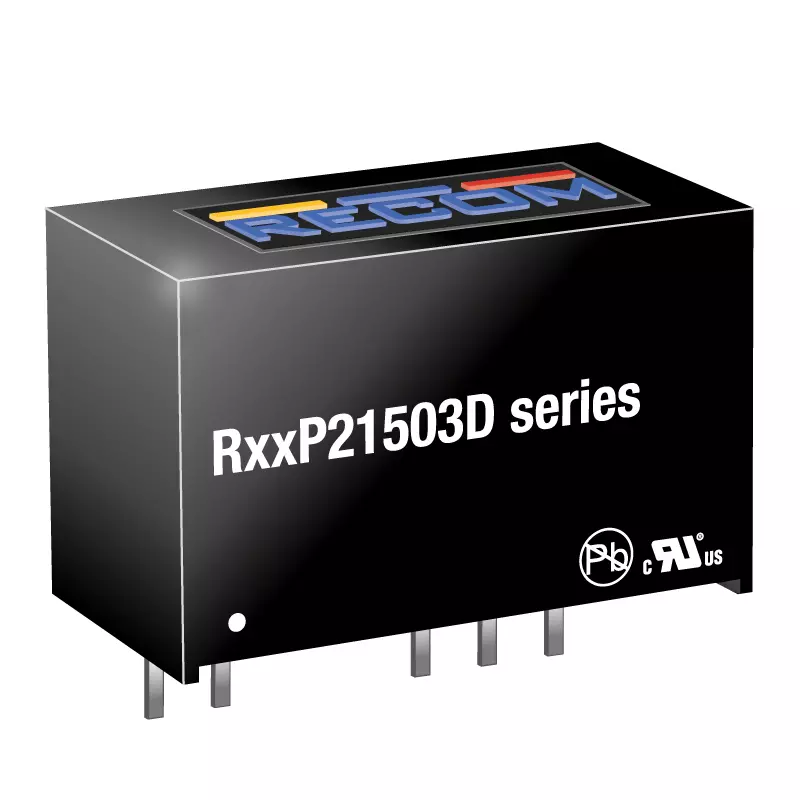
| SiC MOSFETs. The RxxP22005 and RKZ-xx2005 series feature asymmetric outputs of +20V and -5V for efficient SiC MOSFET switching. The RxxP21503 series provides asymmetric outputs of +15V and -3V for second-generation SiC MOSFETs. | GaN HEMTs. High slew-rate GaN drivers reach optimal performance at +6V from RECOM’s RP-xx06 and RxxP06 DC/DC converters with high isolation voltage and low isolation capacitance. For applications with higher noise, RECOM also offers +9V outputs, which can be split via a Zener diode to +6V/-3V to maintain negative gate voltage on turn-off, keeping the gate below the turn-on threshold. |
The table below summarizes recommended DC/DC converters for WBG devices and IGBTs.
|
|
|
The R-REF-HB Half-Bridge Gate-Drive Power Supply Reference Design (RD) consists of a half-bridge suitable for voltages up to 1kVDC and a fully isolated driver stage with isolated power supplies for both low-side and high-side switching transistors. The R-REF01-HB includes two R12P22005D, R12P21503D, R12P21509D, and R12P06S DC/DC converters and can generate gate drive voltages suitable for SiC and GaN devices:
- +20V/-5V
- +15V/-3V or +18V*
- +15V/-9V
- +6V
RECOM engineers closely monitor developments and recommend appropriate gate driver power supplies as new devices are released. For example, Gen IV 35mΩ 650V GaN FETs in TO-247 packages with a Kelvin source pin for optimal switching control can achieve maximum performance with the R-REF01-HB at a +15V/-3V gate drive voltage.
Conclusion
WBG power device technology is rapidly evolving, with new gate drivers continually entering the market to support emerging devices and topologies. RECOM closely tracks these developments, and our engineers can recommend the appropriate power supply solution for your WBG application.
Applications


| Series | |||||||
|---|---|---|---|---|---|---|---|
| 1 |

|
R-REF01-HB
|
|
| |||
| 2 |

|
RKZ-xx2005
|
|
| |||
| 3 |

|
RP-xx06
|
|
| |||
| 4 |

|
RxxP06
|
|
| |||
| 5 |
|
RxxP21503
|
|
| |||
| 6 |

|
RxxP21509
|
|
| |||
| 7 |

|
RxxP22005
|
|
|